Izentis has extensive experience with designing and fabricating micro and nanostructures with a range of applications such as aerospace and neuroscience. We offer a broad range of fabrication services and we are happy to provide a single step or a complete fabrication process for a prototype. We can also fabricate larger structures from metals and plastics for larger devices or packaging. Please contact us with your needs so we can assist you.
- Contact Lithography
- Optical Projection Lithography
- Interference Lithography
- Direct-Write Laser Lithography
- Electron-Beam Lithography
- Spin Coating
- Film Thickness Measurement
- Precision Hot Plate Baking
- Oven Baking
- Oxygen Plasma Resist Stripping
- Reactive-Ion Etching
- Deep Reactive-Ion Etching
- Wet Chemical Processing
- Plasma-Enhanced Chemical Vapor Deposition
- Low-Pressure Chemical Vapor Deposition
- Sputter Deposition
- Oxidation Furnace
- Thermal Annealing
- Electron-Beam Evaporation
- Thermal Evaporation
- Optical Inspection Microscopy
- Electron Beam Microscopy
- Helium-Ion Microscopy
- Fluorescence Microscopy
- Atomic Force Microscopy
- Wafer Curvature Measurement
- Die Saw cutting
- Gold Ball Wire Bonding
- Surface Charge Analyzing
- Chemo-Mechanical Polishing
- Focused Ion Beams
- Ion Implantation
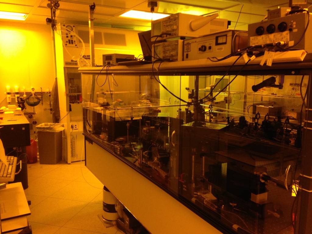
 Interference lithography tool used for patterning gratings.
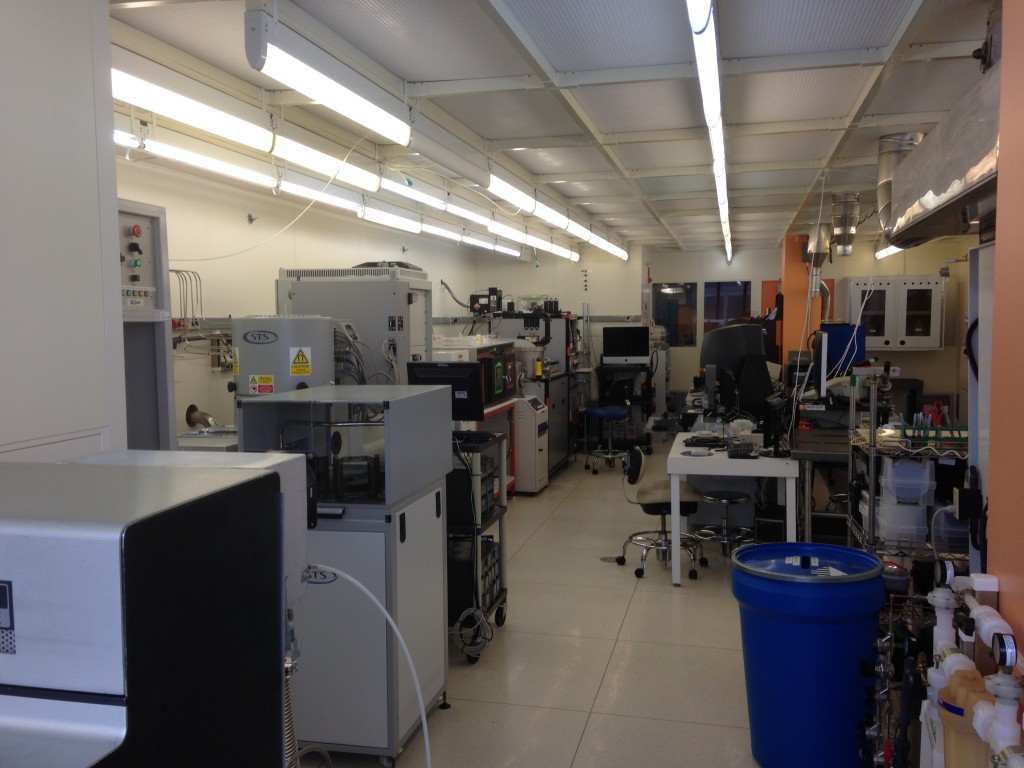
 Plasma etching tools in a clean room used for etching silicon and other common materials in nanofabrication.

